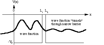
Fig. 1: Electron in a "leaky" box.
Equipment used:
1) Burleigh Instructional STM
Objectives:
A) Demonstration of wave-like nature of electrons by observing a tunnel current
B) Use an STM to image the surface of a (001) plane of graphite and relate the image features to the crystal structure
C) Compare STM results with results of electron diffraction and X-ray diffraction of graphite.
References:
P. A. Tipler, Elementary Modern Physics, Worth Publisher, New York (1992); Section 3-9 (p. 100) and essay on pp. 111-114.
R. A. Serway, C. J. Moses, and C. A. Moyer, Modern Physics, 2nd Edition, Saunders College Publishing, New York (1997); Chapter 6 (p. 228) and essay on pp. 256-262.
K. S. Krane, Modern Physics, Wiley, New York
(1996); Section 5.7, pp. 159-168.
Tunneling Electrons
One of the premises of quantum mechanics is that
particles have a wave-like nature. A wave equation the Schrödinger
equation describes the behavior of these matter waves. The solution of
the Schrödinger equation for a given situation is a wave function
that is related to the probability of finding the particle in a particular
region of space. The most basic situation is an electron confined in space
by infinitely high potential "walls" (electron in a box). For this case
the wave functions vanish at the walls and beyond, which means that the
probability of finding the electron outside the confined space is zero;
the electron is always somewhere inside the box. If we change the
potential to a finite height, the situation changes. Now the wave functions
penetrate somewhat into the potential walls; however, its amplitudes decrease
exponentially and quickly become so small that for all practical purposes
we can call them zero. While the wave function between the walls (i.e.
inside the box) is oscillatory ("wavy"), the wave function in the walls
are non-oscillatory of the form eax.

Fig. 1: Electron in a "leaky" box.
Now consider the potential shown in Fig. 1. This
represents the one-dimensional case of an electron in a box with a thin,
"leaky" wall at x = L1. Initially the electron is
confined inside the box (0 < x < L1). There
the wave function is "wavy". Note, however, that the wave function does
not vanish within the confining wall at L1< x <
L2, but that it decreases exponentially. Since the
wall is very thin there is some amplitude left in the region x > L2,
the wave function of the electron "leaks" outside and hence there is a
small but non-zero probability of finding the electron outside the box.
Classically this could not happen since the total energy of the electron
is lower than the potential barrier. Thus this phenomenon is referred to
as the Tunnel Effect.

A conductor, such as a metal, or graphite, is an
example of electrons in a potential well. A metal crystal consists of atoms
regularly arranged in a lattice. Most of the electrons of the atoms are
bound, but the outermost electrons are free to move inside the crystal.
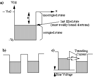
The minimum energy required to remove the most weakly bound electrons is
called the work function you already know about this form Experiment
#1 (Fig. 2a). Bringing two pieces of metal in close proximity without actually
allowing them to touch creates a situation similar to the "leaky" box (Fig.
2b). If the distance between the two conductors is small we can have electrons
from one metal tunnel to the other. However, there is one problem: once
the electron tunnel to the other side, where do they go? Electrons follow
the Pauli exclusion principle which forbids them to share the same quantum
state, i.e. there can be no two electrons with the same quantum numbers.
Thus an electron form the top-most level on the left would not find a free
state after it tunnels to the right, and so tunneling does not occur. Applying
a small bias between the two conductors raises the potential energy of
the electrons in one conductor with respect to the electrons in the other
conductor (Fig. 2c). Now the tunneling electrons end up in unoccupied states,
and a tunneling current can be observed as the electrons from one side
tunnel across to the other side.

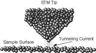
Once established the tunneling current remains constant if the distance between the two conductors stays the same. But because the wave function in the tunneling region between the two conductors has the form eax, the tunneling current is extremely sensitive to changes in distance. Therefore, if we move one of the conductors across the other, the tunneling current will vary with the distance between the two conductors due to bumps and dips at the conductor surface. To achieve a good spatial resolution the probe-conductor is shaped as a very pointy tip which ideally is only one atom wide (Fig. 5). Scanning the tip across a (conducting) sample surface and recording the tunneling current as a function of the tip position results in a "map" of the sample surface as "seen" by the tip. The tip always stays at the same overall height with respect to the sample surface, hence this mode is referred to as the constant height mode. Another way to collect STM image data is the constant current mode. For this mode the distance of the tip to the sample surface is changed such that the resulting tunneling current remains constant. Plotting the distance of the tip to the sample surface vs. the tip position also results in an image of the sample surface.
An STM can thus be realized in principle by using a very sharp tip and moving it a few nanometers above a conducting surface in a controlled fashion. While this may sound simple, a few experimental details remain. In a building, such as Culler Hall, small vibrations are always present from passing vehicles in the street, running motors in the building, people walking in the hall or in the lab. Even minor vibrations have amplitudes of 0.1 to 1 mm, 100 to 1000 times larger than the sample-tip separation. It is obvious that the STM must be isolated from the floor and building vibrations. This may be done by springs or a cushion of compressed air upon which a massive table rests. In our simple experiment vibration isolation is achieved by a granite slab resting on a pressurized inner tube. While the experiment is being performed you should refrain from walking in the lab; even loud conversation will have detrimental effects on the image quality.
In order to obtain atomic resolution the tip must be extremely pointed. Cutting a small wire with regular wire cutters does not make a very fine tip at least not on a microscopic scale. Chemical etching can sharpen the tip radius to about 1000 nm, still much too coarse for a resolution of order 1 nm. Here the experimenter needs, in addition to skill, luck: the etched tip may exhibit roughness of a few atomic dimensions (Fig. 3). The tunneling current from such a tip originates practically from just a few individual atoms; such a tip yields a topographic map with atomic resolution.
The last ingredient for a practical STM is the precise
position control of the tip with respect to the sample surface. The tip
must be capable to move and position itself within a fraction of a nanometer
in x, y, and z directions. This can be accomplished using piezoelectric
ceramics, often referred to as PZT. Piezoelectric ceramics are materials
that expand or contract upon application of a voltage across its ends.Ý
With a tip mounted at the end of a PZT ceramic it is possible to control
the tips movement to 0.1 nm. At the same time the PZT control voltage
can be used to keep track of the tip position. In our experiment a computer
is interfaced with the STM control electronics and draws a topographic
map of the surface that is being scanned. Once an image is stored in the
computers memory in can be manipulated to improve image quality. However,
keep in mind that even the most sophisticated image enhancement software
is worthless if applied to a poor raw image.
For Your Report
2. Note that only alternate atoms in each hexagon are imaged, because the electron wave function projects alternately above or below the plane of hexagons to form the bonds between planes. On your hard copy of the STM image, draw in at least three adjacent hexagons of carbon atoms. To do this you'll have to show the three atoms per hexagon which are not imaged! Don't be fooled by the initial impression that you are seeing the hexagons with an extra atom mysteriously in the center.
3. Now measure directly from your STM image of graphite to obtain the values of the d-spacing respectively between (100) planes, and between (110) planes. Compare with the values for these d-spacings obtained respectively by electron diffraction and by X-ray diffraction.
4. In the X-ray powder diffraction image of graphite, there is no peak corresponding to (001) planes. (True, we did not scan down to the angle 2J where it would be what angle is that? but if we had, we wouldnt have seen the peak!) In fact the overwhelmingly most intense peak corresponds to reflections from the (002) planes. Clearly explain the difference between the (001) planes and the (002) planes. Carefully explain why X-ray diffraction shows reflections from the (002) planes but not the (001) planes. Clearly explain why we can image the (001) planes with the STM.
5. If the (002) reflections are so strong in the X-ray diffraction image, why didn't you see them in your electron diffraction image of graphite? At what angle 2J would reflections from the (002) planes occur if you used an electron accelerating voltage of 4 kV?
6. The electron wavelengths differed from the 1.54
Å wavelength of the copper Ka
X-rays
we used in the X-ray diffraction experiment. Would you therefore expect
the diffraction peak for a given plane in the electron diffraction experiment
to fall at a larger or a smaller value of 2J
than
does the diffraction peak for the same plane in the X-ray diffraction experiment?
Explain.
What would the value of the electron accelerating voltage have to
be to make the electrons deBroglie wavelength equal to 1.54 Å?
I. Startup
A. Turn on Monitor, Computer, and STM Control Electronics.
B. Turn on Printer (Security Block must be installed and printer unplugged from it until
True Image software is loaded)
II. True Image Software for WINDOWS
Commands you enter or pull down (Click on the last of the sequence) are in boldface.
A. Double-click on BURLEIGH icon.
B. File | Load | Open File
C. C:\burleigh\PHY293
Scroll down the list of image file names and double-click on PHY293, or type PHY293
and Click on OK.
D. Collect | Configure
E. "Configure" selects parameters for image.
Set Scan Delay to zero for scanning graphite in constant height mode. Set Zoom
Multiplier to match Magnification (Scan Range) on Control Electronics Console.
It is suggested that for your first scan, you select image size as a square with equal
Scan Range for x and y; each side of the square equals Scan Range/Zoom
Multiplier = 7500 Å/250 = 30 Å.
Note: If you choose (nA) for current mode, the tip will stay a set distance above the macroscopic surface and the scanner records the current as it goes up and down with distance to the microscopic surface. If on the other hand you choose (Å) for topographic mode, the tip is set to keep the current flow constant and so it moves up and down in order to do so. Here the scanner records the height above the surface at which the tip is kept.
Click on OK.
III. STM Tip and Sample
The STM Head is a vibration-isolated rectangular box; through its window you can access the tip and sample, each of which is mounted on a removable carriage. Control Electronics power must be off before changing tip or sample. Before changing either, you must make sure there is plenty of clearance so the tip does not hit the sample while you make adjustments.
A. Remove bell jar.
B. Turn Sample Position Dial down about 1 1/2 turns. (It turns stiffly!)
C. Use tweezers to remove tip carriage.
D. Cut a tip from Pt-Ir wire, and use tweezers to insert tip carriage.
E. Prepare sample, and use tweezers to insert sample carriage.
F. Turn Sample Position Dial up so that sample is about 1 mm from the tip.
G. Replace bell jar.
IV. Control Electronics
A. Monitor Bias Voltage. Set to 0.02 0.10 V for scanning (PZT should read -150 V if not
scanning).
B. Set Reference Current. Set to 0.1 10 nA for graphite.
C. Set Filter Control to MAX (cuts out high frequencies to smooth the image) .
D. For approach set Time Constant to MIN and Gain to MAX.
E. Set X and Y sliders to zero position (locates tip relative to sample).
V. Scanning
A. In software Collect | Scan Unidirectional
B. On Central Electronics Console momentarily press Coarse Retract, and then hold down
Auto Approach to bring tip and sample slowly together. DO NOT use Coarse Approach, or
you will probably crash the tip.
C. Monitor Tunneling Current. With the Sample far away, this current will read zero. As
tunneling begins, this will start to read the same as the preset Reference Current.
D. To scan in constant height mode, set Time Constant to MAX and Gain to MIN.
E. Keep vibration to a minimum by being quiet and still.
F. Watch the image being collected. You may need to make small adjustments to Reference
Current and Bias Voltage. When you are satisfied with the image type H to Halt data
collection. If you choose to abort a scan, type A; this will clear the screen. You can resume
scanning with Collect | Scan Unidirectional.
VI. Saving and Printing the Image
A. If you have not already done so, plug printer cable into Security Block.
B. Press Print Screen key on keyboard.
C. File | Exit
D. You are prompted to save your image file. Click on OK and Yes to overwrite the existing
PHY293.IMG file.
E. Double-click on Paint Shop Pro icon in WINDOWS Program Manager and also when Paint
Shop Pro software loads. Click on OK on information screen.
F. Edit | Paste and your image will appear on the screen.
G. Click on Hand icon and, holding down the mouse button, drag the hand onto your image;
then release the mouse button.
H. File | Print Click on OK to accept default printer. Printing the image will take about
45 minutes.
I. As you gain experience you may learn about processing your image to make it clearer. You
can make measurements of the lattice spacings directly from your image hardcopy; a scale
is included in the image.
VII. Shutdown
A. On the Electronics Control Module, press Coarse Retract until the Tip is well clear of the
Sample.
B. In software, close Paint Shop Pro. Close Burleigh, close Program Manager and exit
WINDOWS.
C. Turn off power to all the electronics.
| This document was last modifed on Wednesday, 27-Sep-2000 16:19:58 EDT
and has been accessed [an error occurred while processing this directive] times. Address
comments and questions to:
|